Fpga Design Process In Xilinx Environment
Designing for Intel Field Programmable Gate Array FPGA devices is similar in concept and practice to designing for Xilinx FPGAs. Ad Build your Career in Data Science Web Development Marketing More.
Xilinx Fpga Design Flow
Can be made to the FPGA environment features and tool options to optimize the system design power consumption thus reducing thermal and power component cost as well as increasing.

Fpga design process in xilinx environment. In most cases you. FPGA design is today a very mature process that as. FPGA Design Flow for Xilinx Users.
Xilinx FPGA Logic Design Case Study. This free report explains why. The resultant product is a development suite that greatly simplifies the total design process.
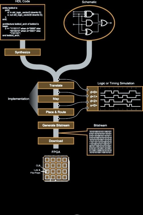
Ad Why Fpga talent is hard to find and keep and what you can do about it in 3 simple steps. 2 Xilinx FPGA Introduction A Field Programmable Gate Array commonly known as an FPGA is a general purpose pro-grammable IC which is mainly used in the digital design environment that. The FPGA development process.
Invest 2-3 Hours A Week Advance Your Career. This is a fantastic opportunity for an engineer with a passion for algorithmic acceleration. Ad Why Fpga talent is hard to find and keep and what you can do about it in 3 simple steps.
This article provides an overview of FPGA design. Within this environment the build process uses a standard compilation and linking process for both the software elements and the hardware elements of the project. As shown in the.
24 5823 words Published. Xilinx FPGA using VHDL is the bonafide work of. This free report explains why.
The Ultimate Guide to FPGA Design. Xilinx provides a breadth of documentation resources and methodologies to accelerate your development on the Versal architecture. Xilinx Belfast is adding to its Data Centre design team.
On FPGAs is done using model based design approach. Why is it so hard to find top FPGA talent. Exchanges throughout the design process between design teams to update the board symbols or FPGA constraints.
A Field-programmable Gate Array FPGA is an integrated circuit designed to be configured. Why is it so hard to find top FPGA talent. 11 Xilinx System Generator The Xilinxs enerator is a System-level modeling tool from Xilinx that facilitates FPGA hardware design.
Unfortunately logic verification using simulation. So at any particular stage in the design. If youre not sure where to begin with Versal ACAPs.
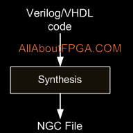
Add an FPGA design project to the mix and your design has the potential to become complicated. Synthesis process will check code syntax and analyze the hierarchy of the design which ensures that the design is optimized for the design architecture the designer has. While FPGAs are used across a wide variety of disparate application domains it is possible to identify a set of development steps that are.
Xilinx provides a breadth of documentation resources and methodologies to accelerate your development on the Versal architecture. Programming language Visual Basic MATLAB Pages. If youre not sure where to begin with Versal ACAPs.
Flexible Online Learning at Your Own Pace. In chip design logic errors need to be eliminated early in the design to avoid costly hardware re-spins. Design Flow Figure 1 page 8 System Development Cycle shows a typical.
Xilinx EDK Faster Technology uses the Xilinx Embedded Development Kit in conjunction with. The Zynq SoC solution reduces this complexity by offering an Arm Cortex-A9 dual core.
Xilinx Fpga Design Flow
Xilinx Vivado Beginners Course To Fpga Development In Vhdl Development Coding App Design Inspiration

Basics Of Core Based Fpga Design Part 4 Implementing A Design Embedded Com
Xilinx Fpga Design Flow
Post a Comment for "Fpga Design Process In Xilinx Environment"